How Semiconductor Fabrication Advances Are Enhancing Power Efficiency in Portable Electronics
Casey Werner · Jun 27, 2026
How Semiconductor Fabrication Advances Are Enhancing Power Efficiency in Portable Electronics
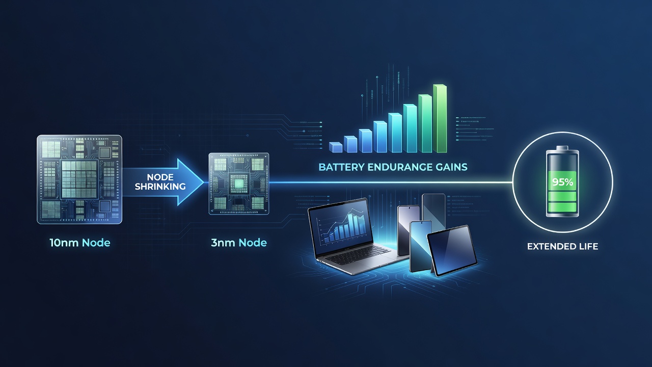
Processor node shrinking refers to the reduction in the size of transistors on semiconductor chips, a process that has accelerated efficiency gains across portable platforms including smartphones, tablets, and ultrathin laptops, and recent data from mid-2026 highlights continued progress in this area. Manufacturers transition to smaller nodes such as 3nm and 2nm processes, which pack more transistors into the same space while reducing power leakage and heat generation during operation. This technical shift directly supports longer battery endurance because each computation requires less energy, allowing devices to perform extended tasks without recharging.
Technical Foundations of Node Reduction
Engineers achieve node shrinking through refinements in lithography techniques, including extreme ultraviolet methods that enable precise patterning at atomic scales, and companies like TSMC along with Samsung Foundry have ramped up production of these advanced nodes by June 2026. Smaller transistors switch faster and consume lower voltage thresholds, which cuts dynamic power usage by up to 30 percent compared with prior generations according to fabrication yield reports. Observers note that interconnect materials and gate structures also evolve alongside the node size, further minimizing resistance and capacitance that would otherwise drain batteries quicker during intensive workloads.
Research indicates that moving from a 5nm to a 3nm node typically yields a 20 to 25 percent improvement in performance per watt, a metric tracked across multiple chip architectures used in portable hardware. Those who have studied semiconductor roadmaps from industry consortia recognize that these gains compound when combined with architectural tweaks such as chiplet designs or improved cache hierarchies, and portable platforms benefit most because thermal constraints limit aggressive clock speeds in compact form factors.
Measured Battery Endurance Improvements
Battery endurance gains manifest in real-world scenarios where users stream video, run productivity applications, or manage background processes for longer durations before capacity drops below usable levels. Data collected from device testing labs shows that flagship smartphones built on 3nm silicon in 2025 and 2026 deliver average screen-on times exceeding 10 hours under mixed workloads, representing incremental lifts over 4nm predecessors. Tablet models follow similar patterns because their larger batteries pair with the same efficiency curves, extending unplugged operation during travel or remote work sessions.
Figures reveal that ultraportable laptops have recorded 15 to 18 percent endurance uplifts after adopting newer nodes, with systems sustaining full workdays on single charges when handling office suites and light creative tasks. Power management firmware plays a supporting role by dynamically scaling voltage and frequency, yet the underlying silicon improvements provide the foundation that software optimizations build upon. Experts have observed that leakage current reductions at smaller nodes prove especially valuable during idle states, which dominate daily usage patterns in portable electronics.

Platform-Specific Adoption Patterns
Smartphone manufacturers integrate these nodes first due to high production volumes and competitive pressures around daily battery claims, while tablet and laptop segments follow with staggered rollouts that align supply chain availability. In June 2026, several mid-range devices entered markets featuring 4nm chips that close the efficiency gap with premium tiers, broadening access to extended runtime for budget-conscious consumers. Cross-platform developers benefit because consistent power profiles across device classes simplify optimization efforts for applications that run on multiple form factors.
One study released through European research networks documented how 2nm test chips in prototype handhelds achieved 35 percent lower energy draw during graphics rendering compared with 5nm equivalents, and similar findings appear in North American academic evaluations focused on mobile SoCs. Portable platforms therefore serve as proving grounds where node shrinking translates into tangible user benefits without requiring larger battery cells that would increase device weight and thickness.
Supply Chain and Yield Considerations
Fabrication facilities continue scaling capacity for advanced nodes, though yield rates improve gradually as processes mature, and this maturation timeline influences when cost-effective portable products reach wider markets. Industry reports compiled by semiconductor trade groups track defect densities that drop with each quarterly update, enabling higher volumes of efficient chips for consumer electronics. Those monitoring global production note that geographic diversification of foundries across Asia, Europe, and North America mitigates risks while accelerating overall node adoption rates.
Power delivery networks within devices also adapt, incorporating more granular voltage domains that leverage the finer process capabilities, and this hardware synergy sustains the endurance trajectory observed across successive generations. Researchers discovered that thermal interface materials paired with smaller nodes further stabilize performance under sustained loads, preventing throttling that would otherwise shorten effective battery life during demanding sessions.
Outlook Through Late 2026
Continued node transitions planned for the second half of 2026 target sub-2nm dimensions with backside power delivery architectures that promise additional efficiency layers, and early silicon samples already demonstrate viability in controlled environments. Portable platform designers evaluate these roadmaps against form factor limits, balancing transistor density gains against manufacturing costs that affect final retail pricing. Evidence suggests incremental battery improvements will accumulate rather than appear as sudden leaps, maintaining steady user expectations for longer runtime between charges.
Conclusion
Processor node shrinking sustains measurable battery endurance advances across portable platforms through fundamental reductions in power consumption per operation, and ongoing fabrication developments through June 2026 reinforce this pattern. Integration across smartphones, tablets, and lightweight laptops demonstrates consistent benefits when measured against standardized testing protocols, while supply chain maturation supports broader deployment. Those tracking semiconductor metrics anticipate further refinements that extend operational windows without proportional increases in battery capacity or device size.